在高电流背板应用中要求实现电路板的带电插拔,这就需要兼具低导通电阻 (在稳态操作期间) 和针对瞬态情况之高安全工作区 (SOA) 的 MOSFET。通常,专为拥有低导通电阻而优化的新式 MOSFET 并不适合高 SOA 热插拔应用。
LTC®4234 是一款针对热插拔 (Hot Swap™) 应用的集成型解决方案,其允许电路板在带电背板上安全地插入和拔出。该器件把一个热插拔控制器、功率 MOSFET 和电流检测电阻器集成在单个封装中,以满足小型化应用的要求。对 MOSFET 的安全工作区进行了生产测试,并保证其能承受热插拔应用中的应力。
LTC4234 的 3.3mΩ 内部 MOSFET 和 0.7mΩ 检测电阻器可支持高达 20A 的负载电流。在该电流水平下,LTC4234 的功率耗散为:
PD = I2 · R = (20A)2 · (3.3mΩ + 0.7mΩ) = 1.6W
对于期望实现较低功率耗散的应用,图 1 所示的电路增设了一个与 LTC4234 的内部 MOSFET 相并联的外部低电阻 MOSFET,旨在把功率耗散降至低于:
PD = I2 · R = (20A)2 · ((3.3mΩ || 0.9mΩ) + 0.7mΩ) = 0.56W
在图 1 所示的 12V 应用中,LTC4234 的 MOSFET 处理的是高漏极至源极电压情况,此时 SOA 是一个主要的关注点。在正常操作期间,当漏极至源极电压较小时,一个 LTC4365 过压 / 欠压电源保护控制器将接通 M1 (其为 0.9mΩ Infineon BSC009NE2LS MOSFET) 以降低总功率耗散,同时实际上消除了对于 SOA 的担忧。
电路运作
在该电路中,LTC4365 在输入电压低于 13.5V 和输出电压高于 10.5V 时接通 M1。由于 M1 的漏极连接至 LTC4234 的 SENSE 引脚,因此所有的电流都流过 LTC4234 的内部 0.7mΩ 检测电阻器。一旦 LTC4234 下拉内部 MOSFET 栅极电压以限制输送至负载的功率,外部 MOSFET 的栅极也将通过低泄漏二极管 D1 (BAR18FILM) 下拉。二极管 D1 的用途是使 LTC4234 的内部 MSOFET 能够在 LTC4365 把外部 MOSFET 保持关断 (当 VIN > 13.5V 或 VOUT < 10.5V 时) 的情况下接通,同时仍然允许 LTC4234 的下拉电路随时将两个 MOSFET 全部关断。建议采用一个低泄漏二极管,以防止 LTC4365 的 GATE 下拉与 LTC4234 的 24µA GATE 上拉电流发生冲突,特别是在二极管漏电流最大的高温情况下。
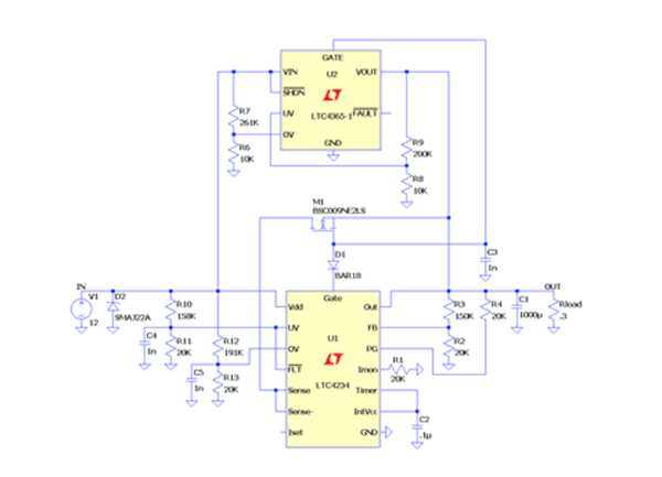
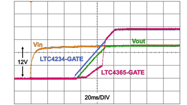
图 2 中的示波器波形显示了当在输入端加电时的电路运行方式。很明显这是一种“阶段式启动”。首先,LTC4234 的内部 MOSFET 在 VIN 上出现电源约 50ms 之后接通,输出电压开始上升。在此期间,当漏极至源极电压很大时,MOSFET SOA 是一个令人担忧的问题,MOSFET M1 处于断开状态。LTC4365 的 GATE (M1 的 GATE) 的缓慢上升是 LTC4365 内部箝位功能电路起作用的结果,该箝位电路负责限制 M1 的栅极至源极电压以保护 MOSFET 的栅极氧化层。在启动阶段结束且输出电压差不多等于输入电压之后,LTC4365 的 GATE 上升以接通外部 MOSFET。M1 起一个“旁路 FET”的作用,可减小从输入至输出的电阻。因此,LTC4234 的内部 3.3mΩ MOSFET 和外部 0.9mΩ MOSFET 在正常操作期间均得到了强化,从而与单单采用 LTC4234 相比功率耗散有所减少。
结论
利用这种方法,我们可以做到两全其美。LTC4234 简化了满足 SOA 要求的棘手任务,而一个专为拥有低导通电阻 (但未必高 SOA) 而优化的外部 MOSFET则降低了 DC 功耗。
作者
Gabino Alonso
Dan Eddleman:Dan Eddleman is an analog engineer with over 15 years of experience at Linear Technology as an IC designer, the Singapore IC Design Center Manager, and an applications engineer.
He began his career at Linear Technology by designing the LTC2923 and LTC2925 Power Supply Tracking Controllers, the LTC4355 High Voltage Dual Ideal Diode-OR, and the LTC1546 Multiprotocol Transceiver. He was also a member of the team that designed the world’s first Power over Ethernet (PoE) Controller, the LTC4255. He holds two patents related to these products.
He subsequently moved to Singapore to manage Linear Technology’s Singapore IC Design Center, overseeing a team of engineers that designed products including Hot Swap controllers, overvoltage protection controllers, DC/DC switched-mode power supply controllers, power monitors, and supercapacitor chargers.
Upon returning to the Milpitas headquarters as an applications engineer, Dan created the Linduino, an Arduino-compatible hardware platform for demonstrating Linear Technology’s I2C- and SPI-based products. The Linduino provides a convenient means to distribute C firmware to customers, while also providing a simple rapid prototyping platform for Linear Technology’s customers.
Additionally, in his role as an applications engineer, he conceived of the LTC2644/LTC2645 PWM to VOUT DACs, and developed the XOR-based address translator circuit used in the LTC4316/LTC4317/LTC4318 I2C/SMBUS Address Translators. He has applied for patents related to both of these products. Dan has also developed multiple reference designs that satisfy the onerous MIL-STD-1275 28V military vehicle specification.
Dan continues to study Safe Operating Area of MOSFETs, and has created software tools and conducts training sessions within Linear Technology related to SOA. His SOAtherm model distributed with LTspice allows customers to simulate MOSFET SOA within their Hot Swap circuit simulations using thermal models that incorporate Spirito runaway.
He received an M.S. in Electrical Engineering from Stanford University and B.S. degrees in Electrical Engineering and Computer Engineering from the University of California, Davis.